
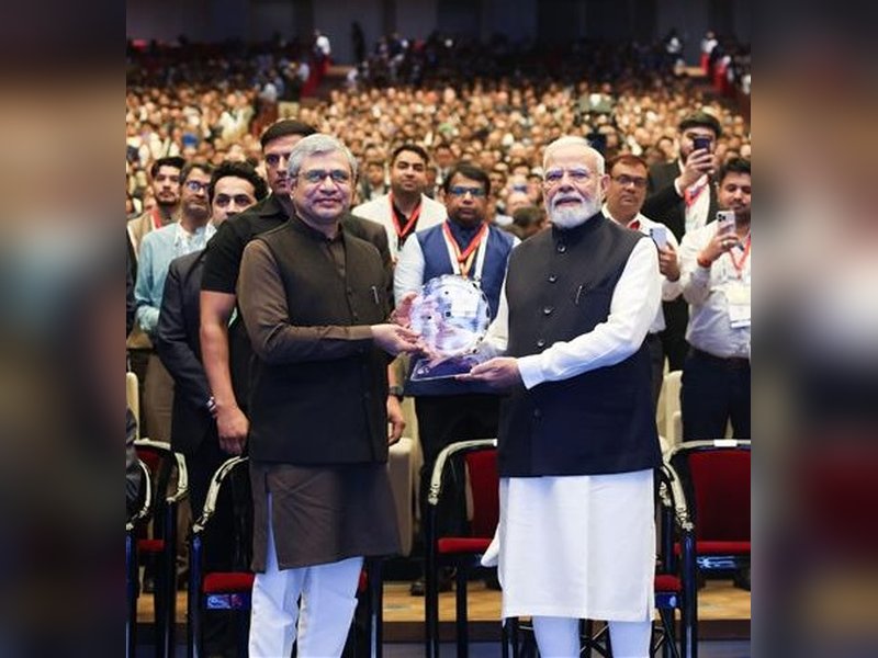
New Delhi, Sep 17 (IANS) Union Minister for Electronics and IT, Ashwini Vaishnaw, said on Thursday that the foundation of the semiconductor industry has been laid in India, and now the industry needs to grow further.
Speaking to IANS on the sidelines of the ‘SEMICON India 2026’ here, the minister said, “whether it is materials, machinery, additional new fabs, ATMP units, design, or talent development — the effort is to develop all of these within India”.
He said that ‘Semicon 2.0’ will build the semiconductor industry over six pillars.
The six pillars under ‘Semicon 2.0’ are Design; Machines and Materials; Setting up more Fabs; Further strengthening the ATMP/OSAT industry; Research and Development; and Talent Development.
“In Semicon 1.0, we had lots of startups trying to see how we can design the chips. We had a goodsuccess. More than 105 startups participated in it, and about 20 of them got VC funding of about Rs 800 crore. That was just the beginning,” said the minister.
IT Secretary S. Krishnan said that this event is much bigger than last year.
“We have close to about 40,000 delegates registered. We have nearly 600-plus companies participating in the exhibition. We have delegates from about 52 countries participating, and more than 300 of these companies participating in the exhibition are overseas companies. This reflects the kind of confidence that the world has in India as a destination for semiconductor manufacturing,” Krishnan told IANS.
Projects supported under Semicon 2.0 will generally have a duration of up to six years, while the scheme will initially remain open for applications for three years. The India Semiconductor Mission (ISM) will be the nodal agency for Semicon 2.0. It will invite applications, undertake technical and financial appraisal, recommend applicants, and oversee implementation.
A mid-term assessment will be conducted after three years of implementation, or as required, to evaluate the scheme’s impact and consider modifications or continuation, it said.
Meanwhile, the government has notified all six pillars of the Semicon 2.0 Scheme, marking a significant step towards strengthening India’s semiconductor design and manufacturing capabilities.
The scheme builds on the momentum generated by the first Semicon India Programme and provides fiscal and infrastructure support across the semiconductor value chain from chip design, fabrication and packaging to equipment, materials, research and development, and talent development.
--IANS
na/